
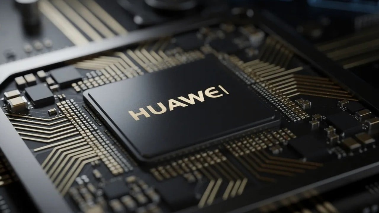
Researchers at Peking University have claimed a breakthrough in microchip design software, purportedly offering critical support to Huawei Technologies as the tech giant attempts to build cutting-edge semiconductors despite US-led trade restrictions.
The innovation, unveiled on Tuesday, comes in the form of a prototype tool for electronic design automation (EDA), according to an announcement by the university’s School of Integrated Circuits. EDA is the highly specialised software that engineers use to design and test microchips before they are manufactured.
Developing a domestic alternative has become a top priority for Beijing because the global EDA market is dominated by Western players such as Synopsys and Cadence Design Systems.
Advertisement
The university’s new EDA tool is compatible with Huawei’s LogicFolding architecture introduced on Monday. The company’s goal is to produce chips by 2031 that match the performance of advanced 1.4-nanometre technology – all without relying on Western chipmaking tools that are subject to China export bans under US export restrictions.
For decades, the global semiconductor industry followed a simple rule: make chips faster by shrinking transistors to pack more onto a silicon wafer. However, after Washington blocked China from buying the advanced lithography machines needed to produce leading-edge chips, Huawei was forced to change its approach.

Instead of making the hardware smaller, Huawei’s new strategy – dubbed the Tau (τ) Scaling Law – focuses on speed. It aims to accelerate how fast electrical signals travel across a chip by reducing resistance and tightening the internal wiring.
Advertisement