
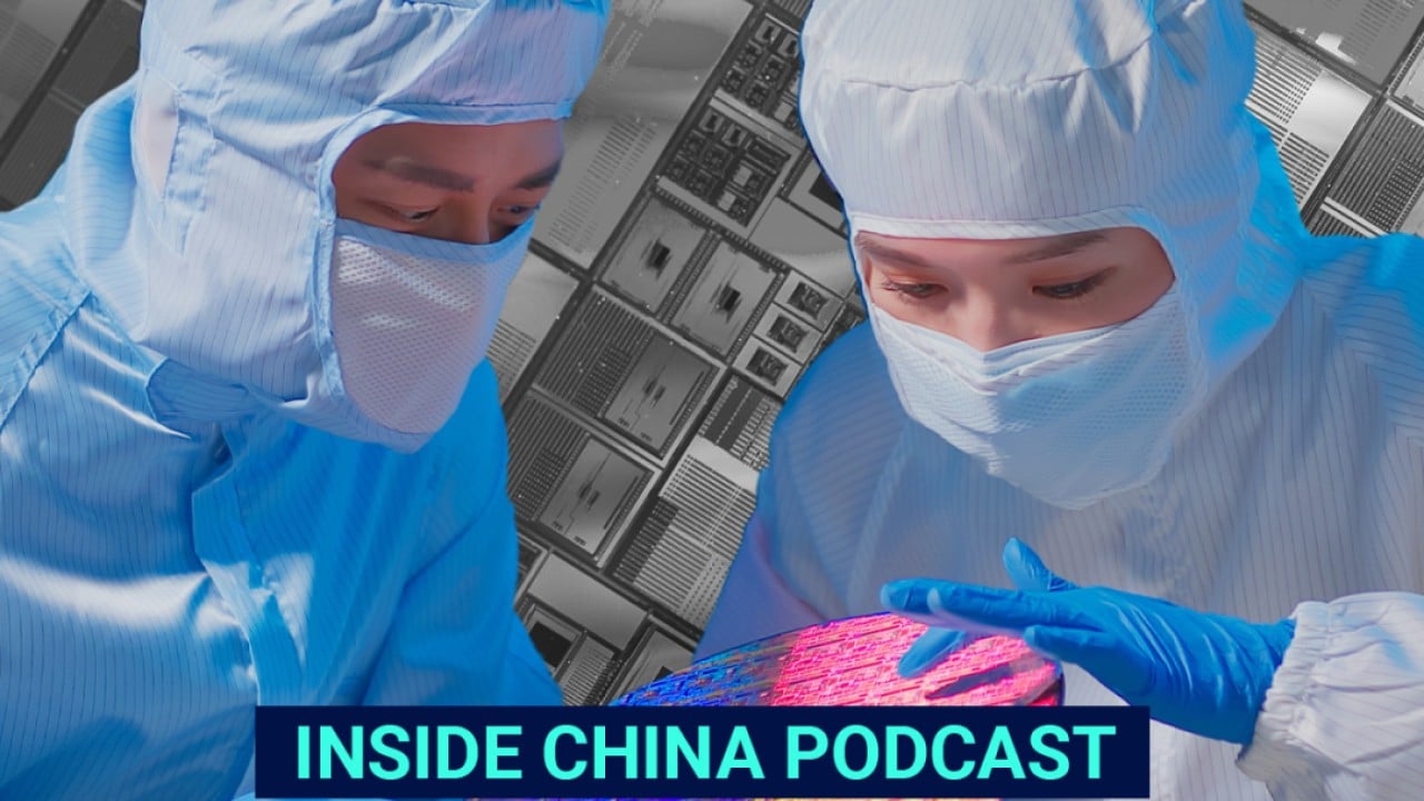
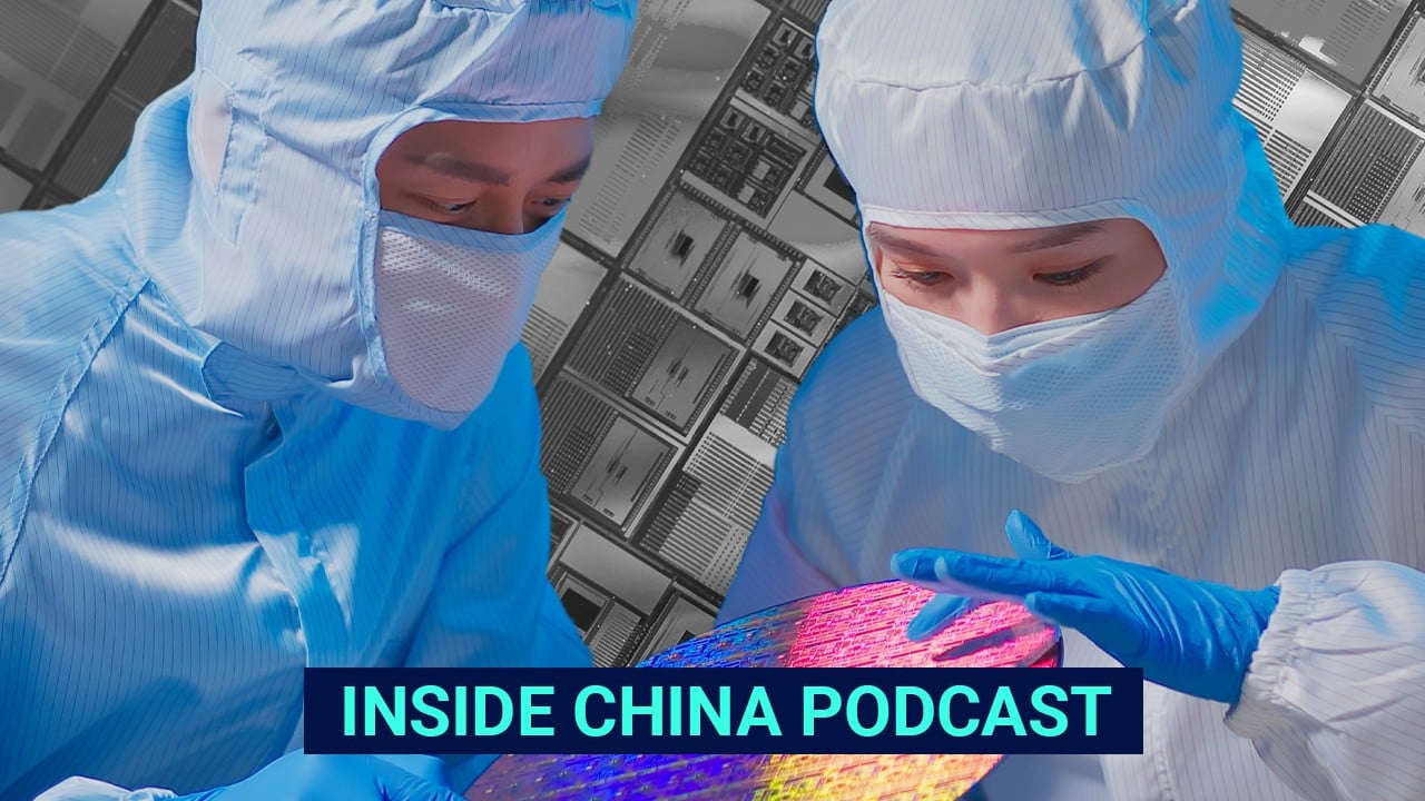
Researchers in Shanghai have come up with a semiconductor chip insulator using an artificial sapphire, a development that could eventually lengthen the battery life of smartphones.
In a paper published in the peer-reviewed journal Nature on Wednesday, the researchers said the atomic-thick sapphire film could be used to build more efficient two-dimensional circuits. The concept was also scalable, they said.
“By constructing complex 2D integrated circuits, the immense potential of 2D materials can be fully unlocked and can lay the groundwork for the next generation of high-performance electronic devices,” said Di Zengfeng, one of the co-leaders of the research team.
Traditional chips, also known as integrated circuits, feature complex, interconnected structures on a silicon wafer substrate.
Transistors within the chips regulate current while dielectric layers made of insulating materials isolate the various conductive layers to prevent current leakage.
Dielectric layers also act as thermal barriers, helping manage heat distribution within the chip.
27:21
Biden’s China tech policy goal: a 10 year handicap
Biden’s China tech policy goal: a 10 year handicap
As chip technology has advanced, the number of transistors in chips has increased, and their arrangement has become more compact.
This evolution has led to higher demands on insulating materials, especially as substrate materials become thinner and close to two-dimensional.
Traditional insulating materials tend to become less effective when reduced to nanometre thickness, resulting in higher power consumption and heat production, which can affect a device’s stability and lifespan.
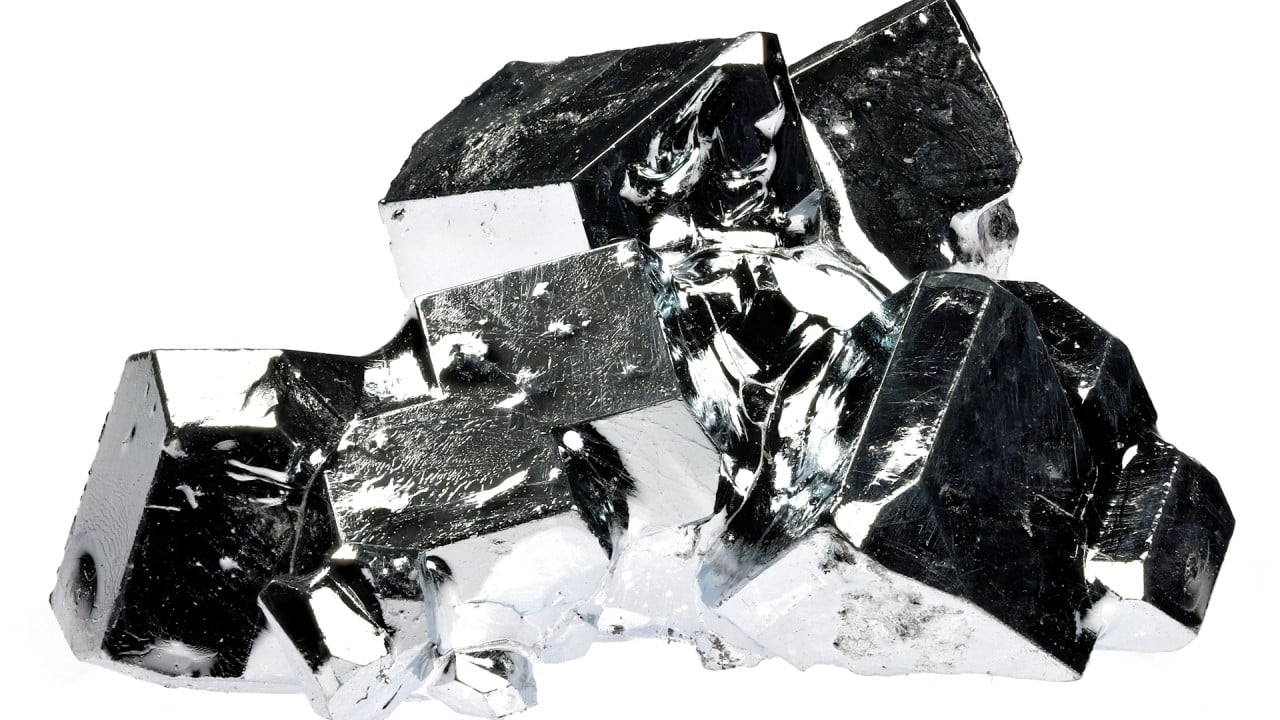
To tackle this problem, a research team led by Di and Tian Ziao – both from the State Key Laboratory of Materials for Integrated Circuits at the Shanghai Institute of Microsystem and Information Technology under the Chinese Academy of Sciences (CAS) – developed a dielectric layer made out of a sapphire film.
The team grew a single-crystal aluminium wafer and then inserted oxygen atoms at room temperature to form a single-crystalline aluminium oxide just 1.25 nanometres thick – a very thin layer of artificial sapphire.

“Although it is artificially synthesised, this film boasts a crystal structure and insulating properties comparable to natural gemstone sapphire,” Tian was quoted as saying in a statement on the CAS website.
The sapphire film was then combined with a two-dimensional substrate of molybdenum disulphide – replacing silicon – to create low-power transistor arrays.
The result pointed to a higher performance integrated circuit.
“These arrays met the International Roadmap for Devices and Systems’ standards for future low-power chips, showing significant improvements in endurance and operational efficiency – laying a foundation for high-performance electronic devices,” the CAS statement quoted Di as saying.
03:36
China restricts critical metal exports following Western semiconductor curbs in latest trade war
China restricts critical metal exports following Western semiconductor curbs in latest trade war
The researchers said the simplicity of the method meant it could be easily scaled to industrial production levels. The manufacturing technique and material characteristics of sapphire film were also compatible with existing silicon-based processes.
According to the paper, the team has demonstrated excellent processing reproducibility and uniformity of the film in a batch of 100 devices.
The researchers said it was a big step towards applying two-dimensional semiconductor materials to industrial settings.
State broadcaster CCTV reported: “This advancement not only holds substantial implications for extending smartphone battery life but also supports the development of low-power chips for artificial intelligence and the Internet of Things.”