
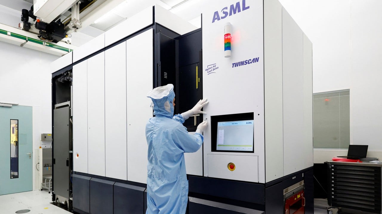
China’s semiconductor industry is continuing to make incremental steps in advancing its domestic lithography tools, according to specifications publicised by the central government, but analysts say the country has yet to make the big leaps it would take to catch up to Dutch firm ASML.
Advertisement
The Ministry of Industry and Information Technology (MIIT), which oversees the country’s chip industry, earlier this month published a list of new tools with the aim of promoting their use by domestic chip makers. While the list contains a slew of tools used in various parts of the manufacturing process – from making integrated circuits to mining and metallurgy – two lithography scanners in particular have caught the attention of international media as a sign of the latest progress being made in the country.
One of the scanners carries a krypton-fluoride (KrF) light source with a 248-nanometre wavelength and an overlay accuracy below 25nm, which is capable of a production resolution of 110nm on 12-inch wafers, according to the MIIT document. The other system uses a more advanced argon fluoride (ArF) light source with a 193nm wavelength and an overlay accuracy below 8nm, supporting a production resolution of 65nm on 12-inch wafers.
Advertisement
The ministry did not specify the manufacturer of the machines, nor how many wafers the machines can produce per hour. More importantly, the MIIT document did not provide details of their capabilities for feature alignment, which could indicate how advanced they might be.
Since last October, Washington’s restrictions on exports to China have specified an allowable level of accuracy for systems using dedicated chuck overlay (DCO), a standard for measuring feature misalignment between two layers exposed by the same machine. A more complex standard called matched-machine overlay checks for alignment of patterns created using different machines. Modern fabrication plants often use different machines to print features on the same wafer to make chips with billions of transistors.
Advertisement