
Today’s computer chips have advanced significantly from 130 transistors per device in the 1970s to 208 billion in 2024 in Nvidia’s latest Grace Blackwell GB200 chip. Defects in semiconductor devices used to be measured in parts per million (ppm), and due to their ever-expanding use in modern vehicles, the market now measures parts per billion (ppb) in the automotive electronics market.
More than 50% of vehicle recalls are associated with failed electronic components, driving the zero-defect race for automotive companies and chip manufacturers.
Wafer processing is a crucial stage in the semiconductor manufacturing process. It involves the creation of integrated circuits (ICs) on silicon wafers through a series of intricate steps, each essential to the functionality and performance of the final semiconductor devices.
Throughout its life cycle, meticulous work is conducted, from growing the crystal boule to wafer dicing, with thorough inspection at each stage to guarantee the selection and utilization of only the finest wafers for chip production.
“Although the process equipment used in semiconductor fabs is extremely sophisticated, there are still manual tasks involved that could benefit from automation standards. A prime example is in wafer dicing, where the commonly practiced manual inspection of sawed wafers is very often lacking digital traceability. By rectifying these minor gaps in the process, the industry can improve quality control and auditing of diced wafers prior to packaging,” said Kevin Fredriksen of PVA Software Production Automation, a company that offers complete high-precision measurement and inspection systems of wafers for the semiconductor industry.
The Life Cycle of a Wafer
The first step in the life of a computer chip begins with manufacturing a mono-crystalline Si boule grown in a Czochralski (CZ) puller. The boule is shaped into 300 mm ingots and then sliced into thin wafers.
Before these wafers are sent to a fab to begin their journey, they are measured using a metrology system known as Scanning Infrared Depolarization (SIRD) to determine if the wafers and their first layers are free of defects and stress that can occur during the growth, grinding, polishing or epitaxy processes. Only the best wafers are selected and used for chip making.
The second step, Patterning, consists of multiple steps to create the transistors, which provide the logic by applying a photoresist, a light-sensitive material, onto the wafer. Then, a Circuit Blueprint is applied using a mask with the desired circuit pattern (like a blueprint for the chip) placed on the wafer. Light is shone through the mask, hardening the exposed photoresist. Once completed, the Image is Developed by chemically washing away the unexposed (soft) photoresist; this creates a patterned layer of photoresist on the wafer.
The third step is Sculpting the Silicon using chemicals and plasma to etch away the silicon where the photoresist isn’t present, forming the basic shapes of the transistors and other components.
Once the etching is complete, plasma strips off the remaining photoresist.
The next step is Doping and Deposition, which introduces impurities into specific areas of the silicon to control its electrical conductivity, creating essential components like transistors. After that, thin films of various materials are deposited onto the wafer using techniques like chemical vapor deposition to create additional circuit elements. These processes are repeated numerous times to build intricate layers of circuits on the wafers.
Once the desired number of layers of transistors is achieved, the wafers must be cut into individual chips before proceeding with individual chip packaging. This step, referred to as dicing, generally entails mechanical sawing or laser cutting.
Despite the advancements in equipment and automation today, some aspects of the fabrication process may still lack sufficient automation and thus could benefit from enhancements to improve inspection quality. One notable gap lies in the crucial inspection process during dicing, which frequently lacks automation and still necessitates manual inspection, assessment and intervention aided by a microscope.
 A new automated visual microscope system simplifies the wafer inspection process using Advanced Visual Inspection (AVI), aligning wafer maps and categorizing defects efficiently.PVA Software Production Automation
Automating Inspection of Diced Wafers
Upon completion of the wafer, specifically when the tip is sealed and it undergoes electrical testing, the wafer proceeds to the sawing machines where it had been positioned on a frame with blue tape for dicing. The pieces remaining on the dicing tape are known as dies.
If the semiconductor fab utilizes Advanced Visual Inspection (AVI) systems to inspect cut wafers for defects – a common practice – then only the first sawed wafer of a lot is placed on an optical microscope. If no AVI equipment is utilized, every diced wafer is inspected manually by an operator.
According to the work instructions, the operator uses the manually controlled microscope to perform a visual inspection of the wafer at several predetermined locations to inspect dicing street quality, die2die distance and chip surface.
“In the average fab, there may be 10 manual microscopes located next to the sawing machines, and operators are constantly going back and forth between the sawing machines and those microscopes to check whether everything is okay on the inspected wafers,” explained Fredriksen. “If there are defects related to the sawing process, the machine is recalibrated before sawing the entire wafer lot.”
If a quality problem is detected, the operator is tasked with marking the chip with an ink dot because normal manual microscopes have no digital wafer map correlation for entering fail die discoveries. In the next step of the process, the pick & place machines identify the chips with ink dots as “fail dies” and leave these chips on the dicing tape.
Now, new technology from companies like PVA Software Production Automation (SPA) is closing the gaps between sawing, inspection and inking through improved automation and inspection. The Coburg-based company specializes in quality inspection systems and production processes in the semiconductor industry.
PVA SPA is a subsidiary of PVA TePla AG, which provides vacuum & nitriding systems, metrology & plasma solutions, scanning acoustic microscopy, crystal growing systems, vacuum processing service and precision research devices.
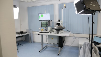
The company’s microscope inspection system is the MI3061 automatic visual microscope for wafer inspection up to 300 mm in size.
The inspection process begins with the operator taking the wafer on frame out of the sawing machine and placing it onto a vacuum transmitted light chuck that holds the frame. The operator triggers the movement of the XY stage with a one-click start. Afterwards the frame label is automatically positioned under the reader where the ID code is read. It starts the lot and loads the correct product recipe and wafer map.
“After manually placing the frame on the chuck, everything is automatic to speed the lot start and wafer map loading process. There is no time to manually enter type or lot information. The system just scans the label, and the wafer is loaded in the correct alignment and predefined first inspection position,” said Fredriksen.
To ensure that the chip position and the corresponding wafer map are synchronized, the system features an automatic alignment and expansion compensation procedure. This automatic function accounts for the expansion of the wafer, which occurs during sawing and can cause a displacement of the XY chip positioning.
“The automatic alignment procedure helps us ensure we have precise positioning even when the chips are shifted,” said Fredriksen. Once this step is completed, the wafer type recipe is used to determine which chip positions should be inspected on the wafer’s front side.
“We have many ways of predefining chip positions and clear rules can be established for a certain type of wafer that should be looked at by the operator,” said Fredriksen.
After the alignment, the operator will be guided through the software to proceed through additional steps in the predefined sequence, including inspecting the chip’s edges. The process is automated but can be controlled by joystick with manual focusing if necessary.
To differentiate between a loose particle and a real mechanical problem the operator can execute an air knife, which is a thin metal pipe that uses compressed air to blow off loose particles precisely from the current inspection position without touching the wafer itself. Previous systems required the use of hand blowers. Instead of viewing the sample through the microscope, the image is displayed on a 27” monitor to simplify detection of any defects.
Each of these steps can be applied to inspect the backside of the wafer (through the dicing tape), as well.
After backgrinding, defects such as scratches, cracks and pits can negatively impact the performance and reliability of fabricated semiconductor devices. SPA actively develops and employs advanced algorithms and even artificial intelligence (AI) within customized machine projects to distinguish between defects and normal expected issues, which can be challenging to differentiate.
If a defect is found, the operator has the possibility to categorize it by utilizing specific error codes which are translated into bincodes in the uploaded wafer map. These codes will then initiate various subsequent actions such as navigating around scratches to guarantee all impacted chips are digitally marked, elevating the chip sample size or progressing to a 100% wafer inspection.
Images of the defective chips are saved and included in a KLARF wafer map output file. On old-fashioned microscopes the operator then has the responsibility to place an ink dot on the affected chips by using a simple hand-held permanent marker. At present, this process in the wafer sawing area is typically conducted manually, with numerous semiconductor fabs continuing to utilize this method. On modern microscopes – such as the MI3061 – applying defect information to dies is done digitally by keying in the error code while inspecting the sample.
As chips decrease in size while wafers increase in size, the task of marking the correct chip with an ink dot becomes increasingly challenging and time-consuming. Nevertheless, this step is crucial as the pick & place machinery in the following stage – especially for automotive products – often relies on this ink dot to detect defective chips for elimination. Neglecting this process could result in defective chips being integrated into electronic devices.
With the MI3061 automatic visual microscope, complete digital traceability is provided by reporting the wafer ID, the recipe name, bincode changes and inspected chip coordinates in a log summary file. This is complemented by a SECS/GEM interface to the host.
The MI3061 compliments AVI inspection, with some semiconductor fabs utilizing the SPA wafer inspection system to reload the result wafer maps to reinspect or review errors the system cannot classify.
To simplify this process, the microscope can automatically move specific chip locations or bincodes into the field of view to inspect unclassifiable anomalies detected by the AVI machine at higher magnification. These errors can be engineered by taking photos and reclassifying the bincode number. This applies to the front and backside of the wafer.
Once wafer inspection on the microscope is complete, the wafer map is sent to the SPA Frame-Inker, a machine that automatically inks the defective wafers and performs a hundred percent ink dot inspection inside the machine.
The framed wafer can then be processed correctly by the pick & place machines, leaving only the skeleton wafer that contains all failed dies.
To assure that no fail chip is accidentally picked up for subsequent processing to packaging, SPA offers a software called PickMapFirewall that overlays an image of the skeleton wafer over the actual skeleton wafer map. An exact match indicates that no defective chips were accidentally picked and postprocessed.
Despite advancements in equipment and automation, certain semiconductor fabrication processes, such as the crucial inspection during dicing, still require manual intervention. This manual process can be inefficient, but new automation technologies like the automatic visual microscope can streamline and improve the process, aiding semiconductor fabs in quality control and productivity.