
In a major leap for the global semiconductor industry, a joint Chinese research team has developed a method that can slash defects in lithography – a critical step in chipmaking – by up to 99 per cent.
Advertisement
The researchers achieved unprecedented clarity by using cryo-electron tomography (cryo-ET) to pinpoint, for the first time, the minute sources of common manufacturing flaws.
The findings, published in the journal Nature Communications on September 30, by Professor Peng Hailin from Peking University in collaboration with researchers from Tsinghua University and the University of Hong Kong, were hailed by reviewers as a “fancy tool” that “would benefit peer researchers and industrial users quite a lot”.
“The team has proposed a solution compatible with existing semiconductor production lines,” Peng said in an interview with Beijing-based Science and Technology Daily published on Monday. “It can reduce lithography defects on 12-inch (30cm) wafers by 99 per cent,” he added, indicating substantial cost benefits to the market.

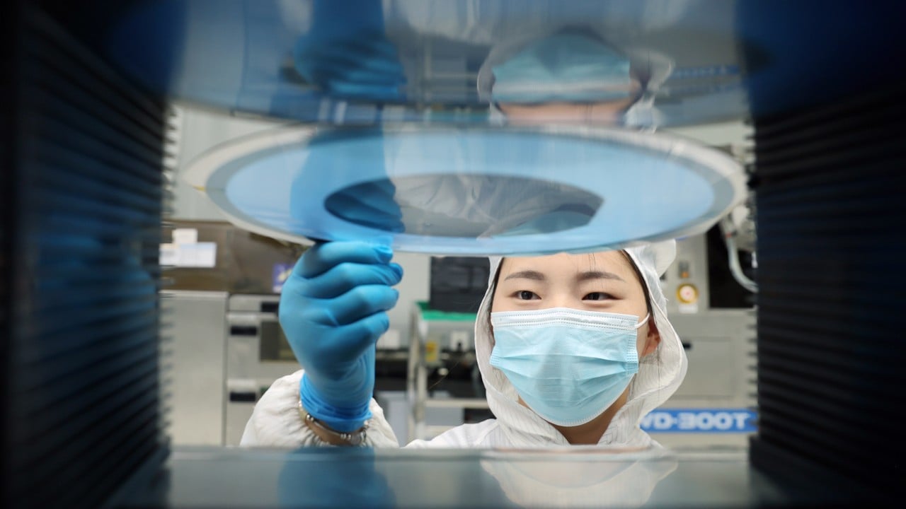
Lithography is one of the most critical steps in chip manufacturing. “It can be understood as ‘printing circuits’ onto semiconductor wafers such as silicon,” Peng said. “Essentially, an ultra-precise ‘projector’ shrinks and transfers pre-designed circuit patterns onto a special film coating the wafer, which is then developed and fixed.”
Advertisement